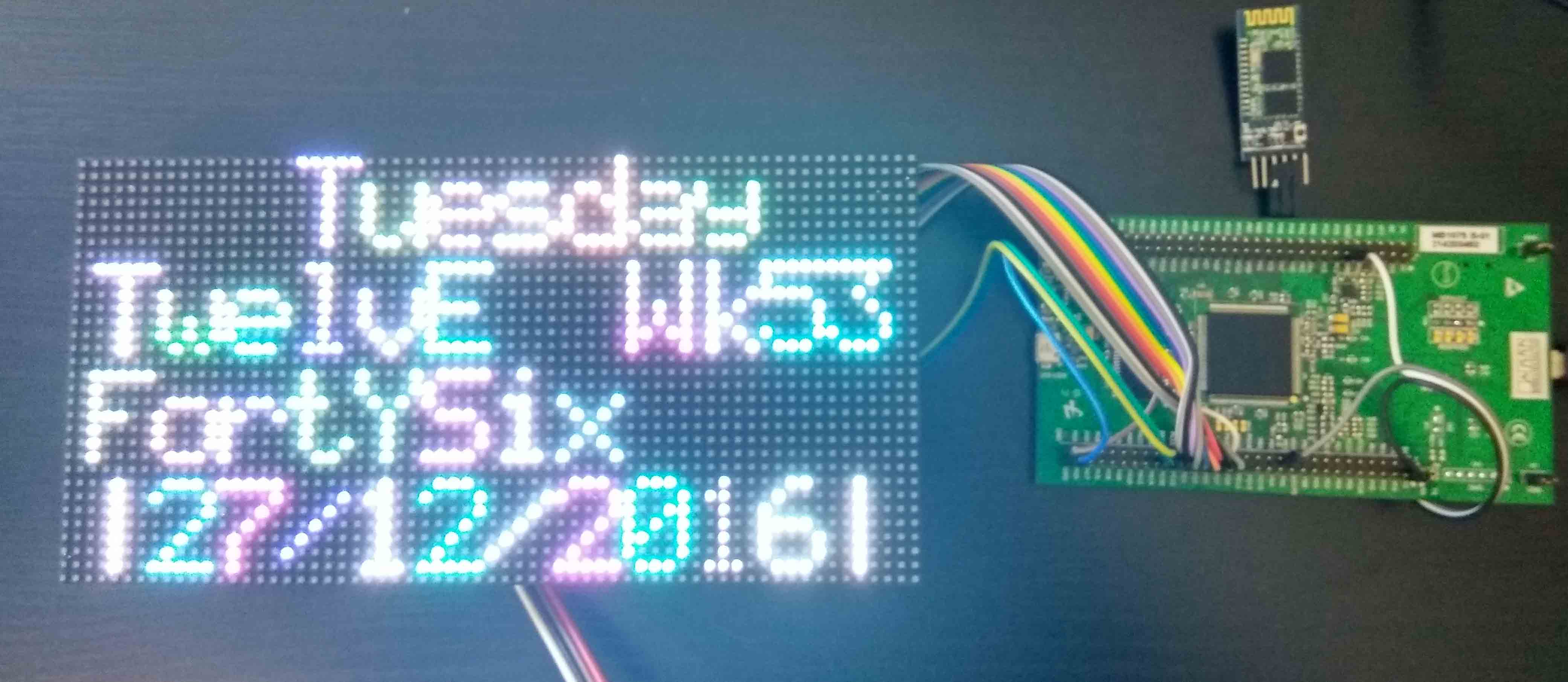
Continuing on the previous work on driving a Dot Matrix Display with an FPGA, the same concept was used to connect an STM32 Discovery board to drive the display. Again, a UART bluetooth module would get data from a server and display it on the matrix.
The Board that was used is an STM32F429 Board. It features a moderately high frequency of 180MHz (top of the line STM32F7 boards have a frequency of 216MHz). However, stil, for such a task, it is low clock, since, compared to FPGAs, all the code is sequential as it will be shown below.
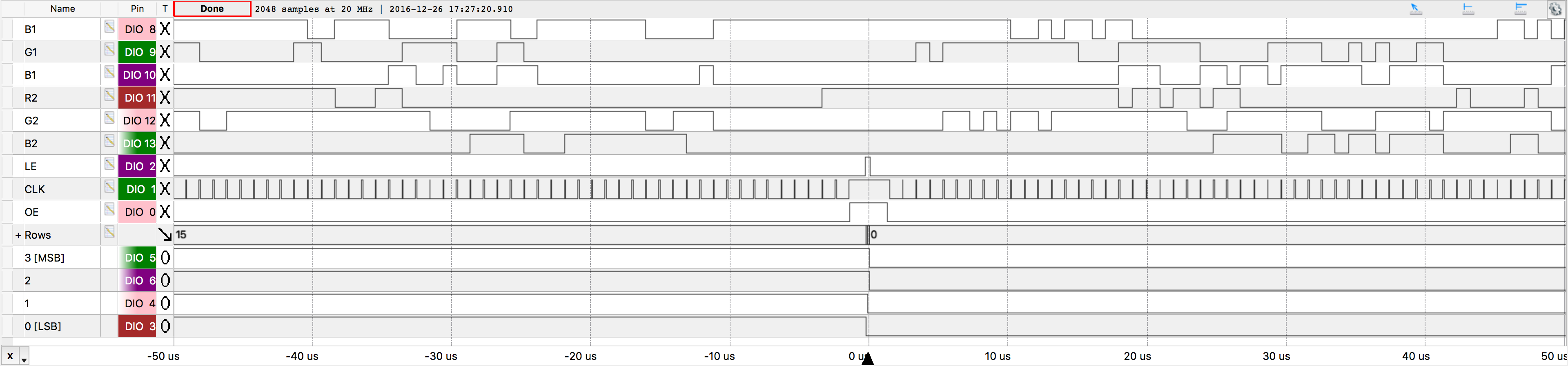
To drive the 64x43 pixel RGBdisplay the following signals need to be supplied:
- Four signals which select the row couple (0-15).
- Three signal couples (RGB1 and RGB2) which select if each LED will be activated or not.
- A clock signal for the shift register.
- A latch enable signal for the shift register.
- An output enable signal.
The GPIO peripherals of the STM32 microcontroller were used. The display operates by driving each row (or more precisely each high/low pair row) individually, using 64 shift registers. After that, the next row pair is driven. In order for this refresh procedure to be invisible to the naked eye, the clock frequency needs to be high. With a PLL clock of 200MHz, a refresh rate of 120FPS were achieved using an FPGA, with 8 bit per color and 64x32 resolution. However, this PLL frequency is even higher than the CPU frequency, meaning the CPU cycle time. As a result, even with such an advanced microcontroller, the refresh rate won't be nowhere as near as the one that was achieved with the FPGA.
The complete code for this project can be found on Github. Other than the GPIO peripherals, the microcontroller uses the UART peripheral to get new data. Since the UART baud rate is low, each transmission would be visible on the display. Since each frame is 64columns x 32rows x 3colors x8bits = 6KB, multiple frames can be stored in the on-board RAM. Pointers are used for the memory bank where the UART stores a new frame as well as for the memory bank from which the controller gets the frame to display. When a new full frame arrives from the UART peripheral, an interrupt is generate to switch banks. Since the processor is busy providing the timings for each pin of the Matrix Display, the DMA peripheral is used to store the data as it arrives from UART. The interrupt is generated by the DMA peripheral.
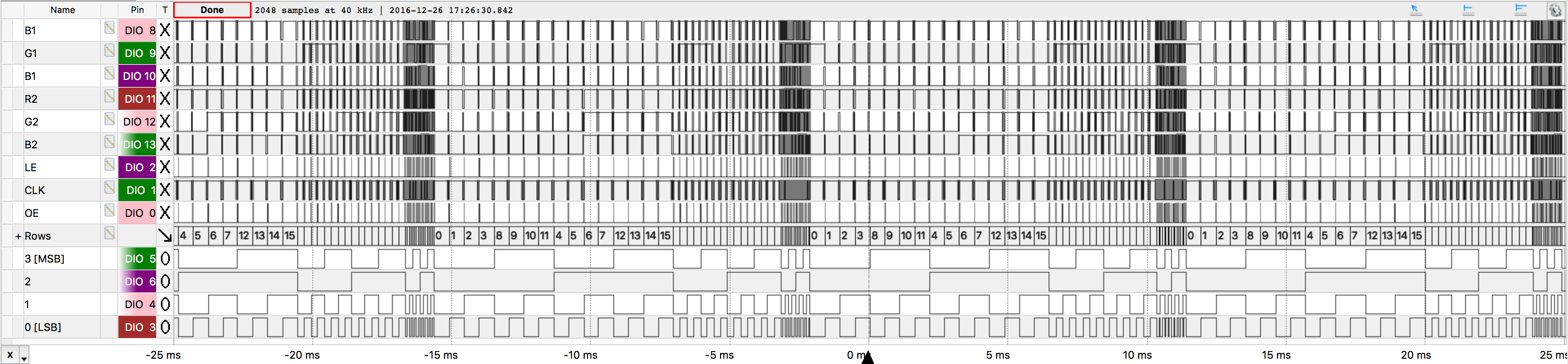
The timing of the different signals can be shown in the images below. As it can be observed, only about 75 frames per second can be achieved, which normally would be more than enough, since for example common VGA CRT displays have a refresh rate of 60Hz. However, since the LEDs switch off instantly, the switching of each row is visible in low frame rate. As a reult, instead of 8 bits color depth (which was the case for the FPGA driver), only 3 bits were achievable with the microcontroller. The different color depths (corresponding to different ON times can be seen as well).
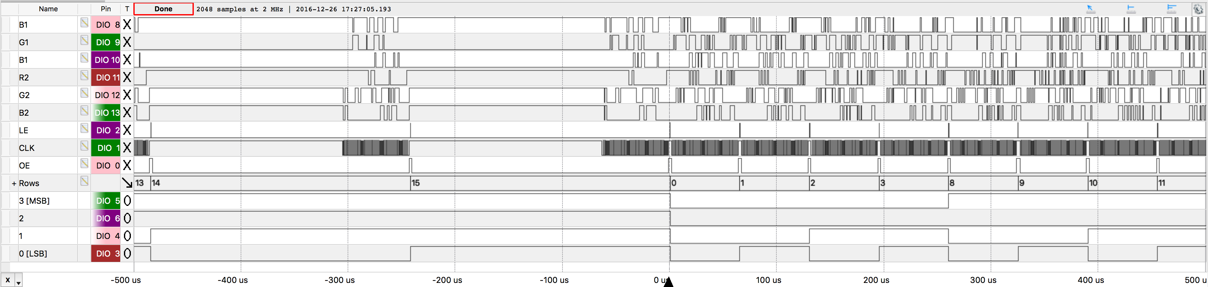
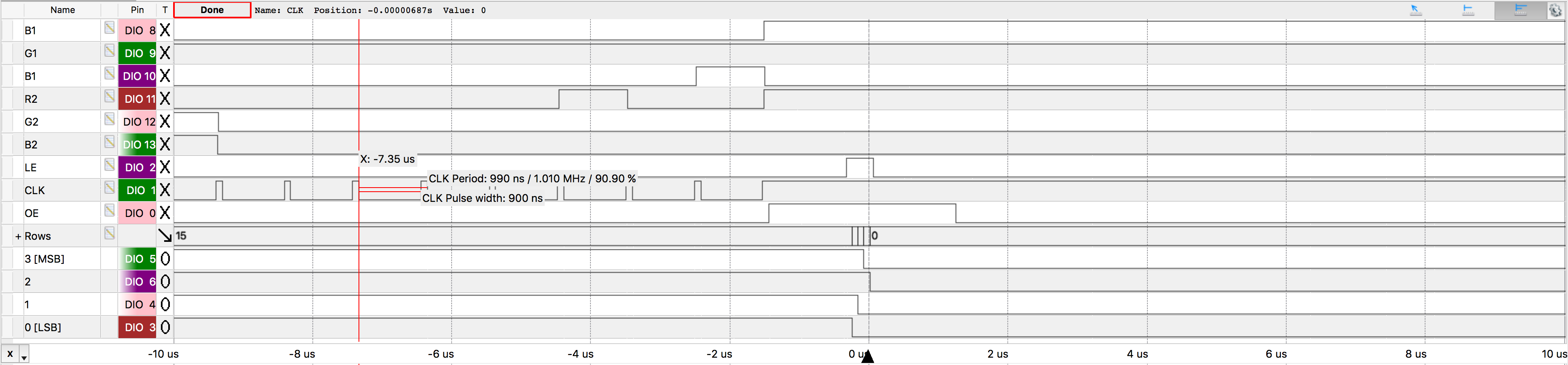
Zooming in even further, the clock rate of the display is shown. The 180MHz microcontroller achieves only 1MHz of clock rate, meaning that on every shift, there are about 180 cycles. The code is not optimized, but the vast difference between this implementation and the FPGA implementation is noted.
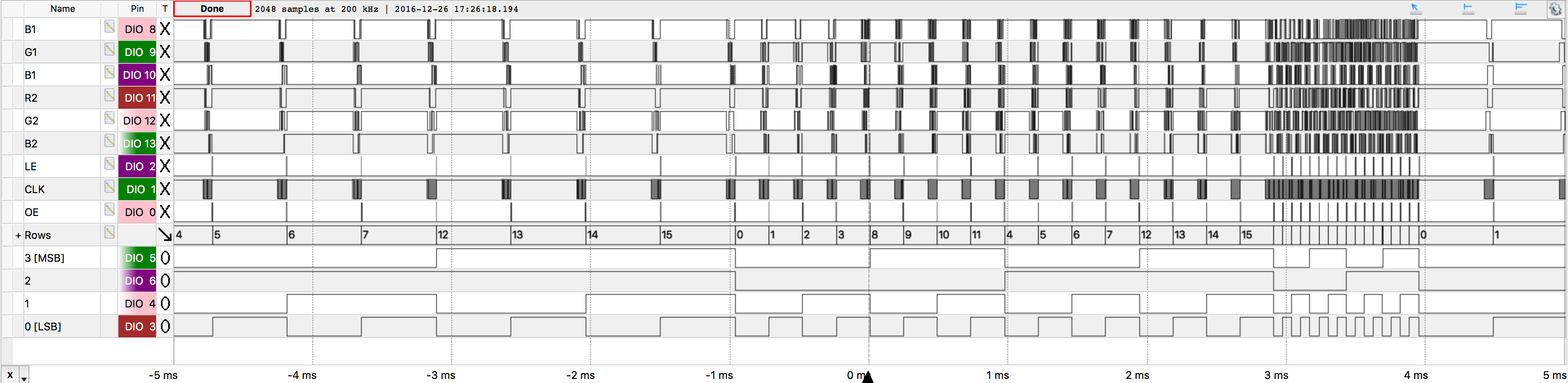
As the row is switched from 15 to 0, each row signal switches sequentially, which is captured in the diagram. Since the OE is high during that time (meaning that the display is momentarily switched off), this is not visible.