PWM Generator on a STM32L152 Discovery
- Details
- Published: Sunday, 20 March 2016 10:36
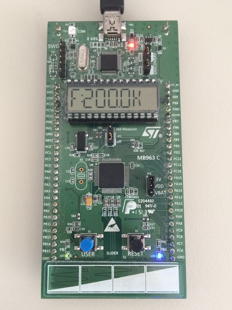
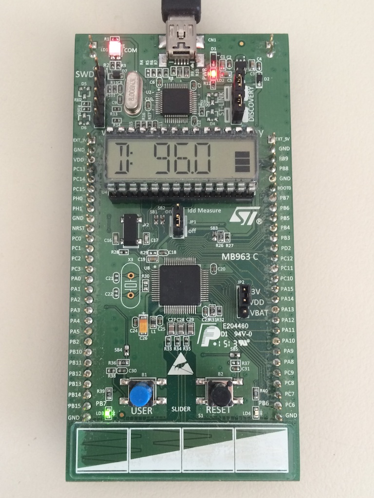
The STM32L152 Discovery is a compact board which includes an LCD display, a touch sensor (linear or four keys), a push button and two LEDs. Combining all of the above, a compact PWM generator can be made with variable frequency and duty cycle.
The LCD will display the current value to be adjusted meaning either the frequency or duty cycle of the pulse. To cycle between the two settings, the push button will be used. The values will be set using the touch sensor. Finally, the pulse will be output to the green LED in order to show the actual duty cycle (via the LED intensity). The second LED will be used to show which of the two values is currently adjusted (it will also be shown in the display).
So, the timer that will be used is TIM4 and Channel 2, in order to output the PWM pulse to the blue LED (Port PB7). A standard initialization function is first run, meaning starting the timebase, the output channel and finally connecting the channel 2 output to port PB7:
void TIM4Init()
{
TIM_TimeBaseInitTypeDef TIM_InitStruct;
TIM_OCInitTypeDef TIM_OCInitStruct;
GPIO_InitTypeDef GPIO_InitStructure;

RCC_APB1PeriphClockCmd(RCC_APB1Periph_TIM4,ENABLE);
TIM_InitStruct.TIM_ClockDivision = TIM_CKD_DIV1 ;
TIM_InitStruct.TIM_CounterMode = TIM_CounterMode_Up;
TIM_InitStruct.TIM_Period = 32000;
TIM_InitStruct.TIM_Prescaler = 1;
TIM_TimeBaseInit(TIM4, &TIM_InitStruct);
TIM_Cmd(TIM4, ENABLE);

TIM_OCInitStruct.TIM_OCMode = TIM_OCMode_PWM1;
TIM_OCInitStruct.TIM_Pulse = 100;
TIM_OCInitStruct.TIM_OutputState = TIM_OutputState_Enable;
TIM_OCInitStruct.TIM_OCPolarity = TIM_OCPolarity_High;
TIM_OC2Init(TIM4, &TIM_OCInitStruct);

RCC_AHBPeriphClockCmd(RCC_AHBPeriph_GPIOB, ENABLE);
GPIO_InitStructure.GPIO_Mode = GPIO_Mode_AF;
GPIO_InitStructure.GPIO_OType = GPIO_OType_PP;
GPIO_InitStructure.GPIO_Pin = GPIO_Pin_7;
GPIO_InitStructure.GPIO_PuPd = GPIO_PuPd_NOPULL;
GPIO_InitStructure.GPIO_Speed = GPIO_Speed_10MHz;
GPIO_Init(GPIOB, &GPIO_InitStructure);

TIM_OC2PreloadConfig(TIM4, TIM_OCPreload_Enable);
GPIO_PinAFConfig(GPIOB, GPIO_PinSource7, GPIO_AF_TIM4);
UpdatePWM(frequency, duty);
}
Next, an easy backend to change the frequency and duty cycle must be used. The function UpdatePWM takes two operands (frequency and duty cycle) and appropriately configures TIM4. Since the L1 microcontroller can run in different clock frequency configurations, the "SystemCoreClock" variable used, which is set in the system source file (assuming that the APB1 Prescaler is 1):
void UpdatePWM(double frequency, double duty)
{
//frequency in Hz, duty 0-100.0
long int ratio;

ratio = (long)SystemCoreClock/frequency;
TIM4->PSC = (int)(ratio/0xFFFF);

ratio = ((long)SystemCoreClock/(TIM4->PSC+1));
TIM4->ARR = (int)(ratio/frequency)-1;

TIM4->CCR2 = (int)((TIM4->ARR+1)*duty)/100-1;
}
To update the LCD Display, the provided function LCD_GLASS_WriteChar is used for each character, whereas, a custom bargraph function is written to update the bargraph as a percentage value:
void UpdateDisplay(void)
{
bargraph((int) duty, 100);
if (state==FREQ) sprintf(displaystring,"f%4.2dk", (int) (10*frequency));
if (state==DUTY) sprintf(displaystring,"d%4.2d%%", (int) (10*duty));
 LCD_GLASS_WriteChar((unsigned char *)displaystring + 0, 0, COLUMN_ON, 1);
 LCD_GLASS_WriteChar((unsigned char *)displaystring + 1, 0, 0, 2);
 LCD_GLASS_WriteChar((unsigned char *)displaystring + 2, 0, 0, 3);
 LCD_GLASS_WriteChar((unsigned char *)displaystring + 3, POINT_ON, 0, 4);
 LCD_GLASS_WriteChar((unsigned char *)displaystring + 4, 0, 0, 5);
 LCD_GLASS_WriteChar((unsigned char *)displaystring + 5, 0, 0, 6);
}
void bargraph(int value, int max)
{
double percentage=(double)value/(double)max;
BAR0_OFF;
BAR1_OFF;
BAR2_OFF;
BAR3_OFF;
if (percentage>0.25) BAR0_ON;
if (percentage>=0.5) BAR1_ON;
if (percentage>=0.75) BAR2_ON;
if (percentage==1) BAR3_ON;
LCD_bar();
}
Finally, the touch sensor value is read using the provided STMTouch driver.
The full project of the PWM Generator for the STM32L152 Discovery can be found on my Github page.

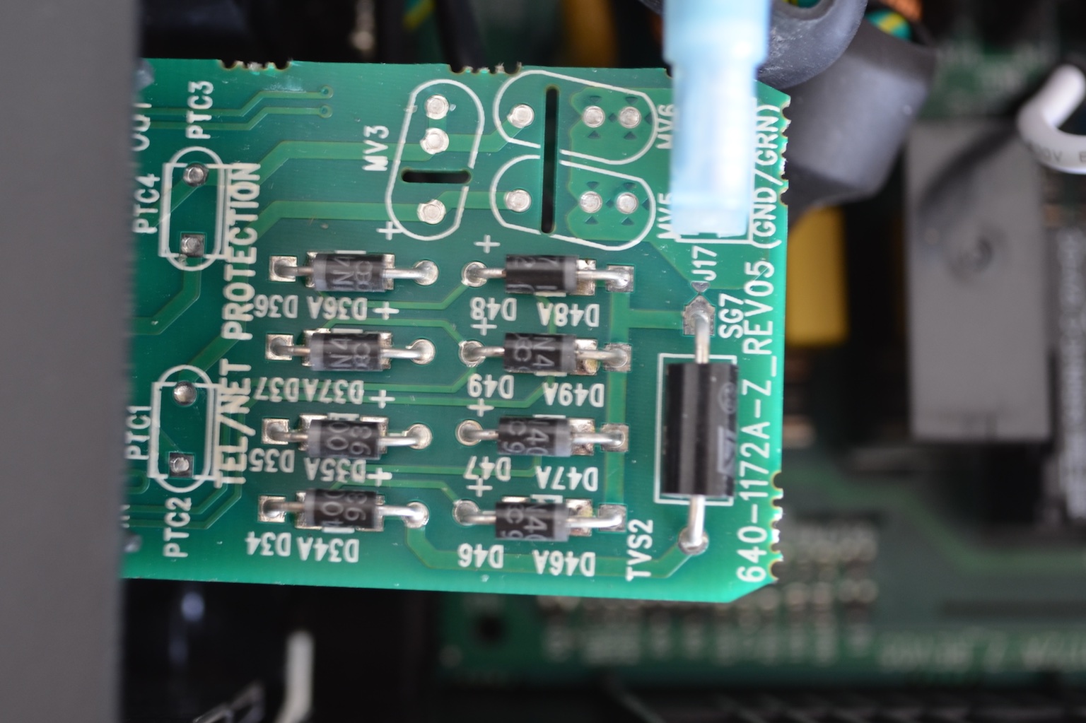
 A separate board is used for the telephone line protection.